G80
Overview
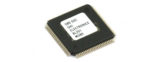
The G80 SoC is a low-cost System on Chip part of the GHI Electronics SurfaceMount Compute Modules (SCM) line. This modules can be programmed in .NET C# and Visual Basic using .NET Micro Framework.
Tip
Not recommended for new designs, consider SITCore System on Chip.
Ordering Part Number
- G80 SoC: G80SC-SM-501
- G80 Dev Board: G80DB-SM-483
Specifications
| Spec | Value |
|---|---|
| Processor | STM32F427VGT6 |
| Speed | 180 MHz |
| Internal RAM | 256 KByte (SRAM) |
| Internal Flash | 1 MByte |
| Package | LQFP100 14 x 14 mm |
| Temperature Range | -40C to +85C |
Note: Resources are shared between your application and the operating system.
Features
- .NET Micro Framework
- RoHS Lead Free
- 180 MHz ARM Cortex-M4 STM32F427VGT6
- 156 KBytes available RAM
- 256 KBytes available flash
- 78 GPIO
- 16 interrupt capable GPIO
- 2 SPI
- 1 I2C
- 4 UART
- 2 CAN
- 26 PWM
- 16 12-bit analog input
- 4-bit SD/MMC memory card interface
- Low power modes
- LQFP6100 14 x 14 mm
- RTC
- Watchdog
- Threading
- USB host
- USB client
- TCP/IP with SSL
- Full .NET socket interface
- Ethernet
- PPP
- Graphics
- Images
- Fonts
- Controls
- File System
- Full .NET file interface
- SD cards
- USB drives
- Native extensions
- Runtime Loadable Procedures
- Device register access
- Signal controls
- Generation
- Capture
- Pulse measurement
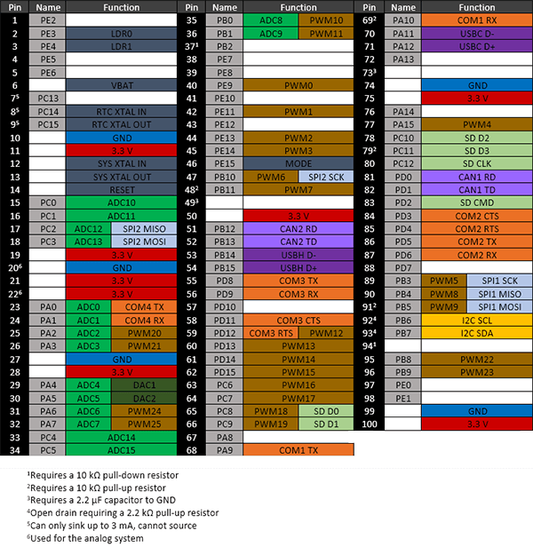
G80 Pinout
Many signals on the G80 are multiplexed to offer multiple functions on a single pin. Developers can decide on the pin functionality to be used through the provided libraries. Any pin with no name, function, or note must be left unconnected.
Footprint
The chip is standard LQFP100 14x14mm. See the STM32F427VGT6 datasheet for exact footprint.
Device Startup
The G80 is held in reset when the reset pin is low. Releasing it will begin the system startup process.
There are three different components of the device firmware:
- GHI Electronics Bootloader: initializes the system, updates NETMF firmware when needed, and executes NETMF.
- NETMF Firmware: loads, debugs, and executes the managed application.
- Managed application: the program developed by the customer.
Which components get executed on startup can be control by manipulating the LDR0 pin. It is pulled high on startup. When low, the device waits in the GHI Electronics Bootloader. Otherwise, the managed application is executed. LDR1 is reserved for future use.
Additionally, the communications interface between the host PC and the G80 is selected on startup through the MODE pin, which is pulled high on startup. The USB interface is selected when MODE is high and UART1 is selected when MODE is low.
The above discussed functions of LDR0, LDR1, and MODE are only during startup. After startup, they return to the default GPIO state and are available to use as GPIO in the user application
.NET Micro Framework
NETMF provides a way to program the G80 in C# or Visual Basic from the Microsoft Visual Studio integrated development environment. To get started you must first install the firmware on the G80 (instructions below) and then go to the NETMF Getting Started page for instructions.
Loading the Firmware
- Activate the bootloader, hold the LDR0 signal low while resetting the board.
- Open the FEZ Config tool and follow the instructions.
You can also update the firmware manually. See GHI Electronics Bootloader manually.
Start Coding
Now that you have installed the firmware on the G80, you can setup your host computer and start programming. Go to the NETMF Getting Started page for instructions.
Datasheet
This documentation page replaced the legacy datasheet PDF but it is here for reference.
CAN Bit Timing Settings
The following CAN bit timing parameters were calculated for a G80 driving the TJA1050T CAN driver chip. See the CAN Tutorial for more information.
| Baud | Propagation | Phase1 | Phase2 | Baudrate Prescaler | Synchronization Jump Width | Use Multi Bit Sampling | Sample Point | Max Osc. Tolerance | Max Cable Length |
|---|---|---|---|---|---|---|---|---|---|
| 33.333K | 1 | 12 | 2 | 90 | 1 | False | 86.7% | 0.33% | 2145M |
| 83.333K | 1 | 12 | 2 | 36 | 1 | False | 86.7% | 0.33% | 825M |
| 125K | 1 | 12 | 2 | 24 | 1 | False | 86.7% | 0.33% | 531M |
| 250K | 1 | 12 | 2 | 12 | 1 | False | 86.7% | 0.33% | 238M |
| 500K | 1 | 12 | 2 | 6 | 1 | False | 86.7% | 0.33% | 91M |
| 1M | 1 | 12 | 2 | 3 | 1 | False | 86.7% | 0.33% | 18M |
Note: Maximum Oscillator Tolerance and Maximum Cable Length are theoretical maximums and must be tested to ensure reliability.
Design Considerations
Required Pins
Exposing the following pins is required in every design to enable device programming, updates, and recovery:
- LDR0
- LDR1
- Reset
- Desired debug interface(s)
- MODE if required to select a debug interface
Power Supply
A typical clean power source, suited for digital circuitry, is needed to power the G80. Voltages should be within at least 10% of the needed voltage. Decoupling capacitors of 0.1 μF are needed near every power pin. Additionally, a large capacitor, typically 47 μF, should be near the G80 if the power supply is more than few inches away.
Crystals
The G80 requires an external 12 MHz crystal and associated circuitry to function. For the RTC to function, a 32,768 Hz crystal and circuitry are required. Please see the processor’s documentation for advanced information.
Interrupt Pins
Interrupts are only available on 16 pins at any given time. Of those 16 pins, the pin number must be unique. For example: PA1 and PB1 cannot both be used as interrupts at the same time, but PA1 and PB2 can.
Reset
The reset pin is not pulled in any direction. Designs must be sure to use an appropriate pull-up resistor.
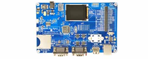
G80 Development Board
The G80 Dev Board is an excellent starting point and reference design for anyone interested in evaluating and developing with the G80.
You can also visit our main website at main website and our community forum.