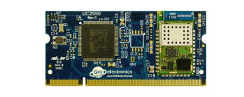
UC2550
Overview
The efficiency of our UC2550 makes it ideal for low power applications. It is also our lowest cost UCM and offers a large complement of peripherals.
Ordering Part Number
| Model Number | WiFi | External QSPI Flash |
|---|---|---|
| UC2550-13NNN | no | optional |
| UC2550-13NNW | yes | optional |
Specifications
| Specs | Value |
|---|---|
| Processor | STM STM32F413 32-bit ARM Cortex-M4 |
| Speed | 100 MHz |
| Internal RAM | 320 KByte (SRAM) |
| Internal Flash | 1 MByte |
| External RAM | 0 KByte |
| External Flash | Up to 4 MByte (QSPI) |
| Dimensions | 67.7 x 31.7 x 3.2 mm |
Note: Not all memory will be available for your application.
Peripherals
This table lists the available peripherals. The "overall" column shows the available pins if the design did not follow the UCM standard.
| Peripheral | UCM Standard | Overall |
|---|---|---|
| UART | 4 | 9 (including HS) |
| UART HS | 2 | 2 |
| I2C | 2 | 2 |
| SPI | 2 | 3 |
| CAN | 2 | 2 |
| SDIO | 1 | 1 |
| ADC | 8 | 15 |
| PWM | 8 | 27 |
| GPIO | 10 | 67 |
| IRQ | 4 | 67 |
| USB Client | Supported | Supported |
| USB Host | Not supported | Not supported |
| LCD | Not supported | Not supported |
| Ethernet PHY | Not supported | Not supported |
| WiFi | Supported | Supported |
| Camera | Not supported | Not supported |
| VBAT | Supported | Supported |
| JTAG | SWD | SWD |
Development Options
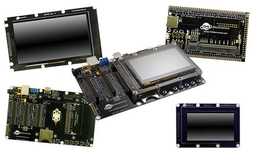
The UCM development options can greatly simplify the process of building a product or prototype using the UC2550. Options include a development board and displays which can get you programming in minutes.
Tip
We are assuming you are using the UCM Development Board for all instructions provided.
.NET Micro Framework
NETMF provides a way to program the G30 in C# or Visual Basic from the Microsoft Visual Studio integrated development environment. To get started you must first install the NETMFfirmware (instructions below) and then go to the NETMF Getting Started page for instructions.
Loading Bootloader v2
- Download the UC2550 bootloader here.
- Connect your device to the USB client port.
- Put the board in DFU mode: Hold the SYS A pin low and press/release the reset button. Wait for a second then release SYS A. Windows Device Manager will now show "STM Device in DFU Mode" under the 'Universal Serial Bus controller' TAB.
- This is a DFU file, upload it like you would any other DFU file. See STMicroelectronics documentation for details.
Loading the Firmware
- Activate the bootloader, hold the LDR0 signal low while resetting the board.
- Open FEZ Config tool and follow the instructions.
Start Coding
Now that you have installed the bootloader and firmware on the UC2550, you can setup your host computer and start programming. Go to the NETMF Getting Started page for instructions.
Schematic
The schematic for the UC2550 can be found here.
Customization
We also offer customized, non-stock versions of our SoMs. Many options are available, such as various sizes of external QSPI flash. Please contact us for details. We will always do our best to provide you with a module to fit your exact needs.
Pin Assignments
| SO-DIMM Pin | Universal Compute Standard | Function Name |
|---|---|---|
| 1 | AGND | AGND |
| 2 | Ethernet TX- | |
| 3 | Module Specific 1 | (WiFi PIN14) WiFi Power LED |
| 4 | Ethernet TX+ | |
| 5 | Analog VREF- | Analog VREF- |
| 6 | Ethernet RX- | |
| 7 | Reserved | |
| 8 | Ethernet RX+ | |
| 9 | Reserved | |
| 10 | Indicator A | (WiFi PIN15) WiFi Link Up LED |
| 11 | Indicator B | (WiFi PIN5) WiFi Running (Blink) LED |
| 12 | Reserved | |
| 13 | GND | GND |
| 14 | DCMI D0 | |
| 15 | DCMI D1 | |
| 16 | DCMI D2 | |
| 17 | DCMI D3 | |
| 18 | DCMI D4 | |
| 19 | DCMI D5 | |
| 20 | Analog 3.3V | Analog 3.3V |
| 21 | DCMI D6 | |
| 22 | DCMI D7 | |
| 23 | DCMI VSYNC | |
| 24 | DCMI HSYNC | |
| 25 | DCMI PIXCLK | |
| 26 | DCMI XCLK | |
| 27 | GND | GND |
| 28 | PWM E | PE5, TIM9 CH1 |
| 29 | PWM F | PE6, TIM9 CH2 |
| 30 | PWM G | PB14, TIM12 CH1 |
| 31 | PWM H | PB15, TIM12 CH2 |
| 32 | Analog VREF+ | Analog VREF+ |
| 33 | Reserved | |
| 34 | 5V | |
| 35 | Module Specific 4 | (WiFi PIN13) |
| 36 | Module Specific 5 | (WiFi PIN16) |
| 37 | Module Specific 6 | (WiFi PIN22) |
| 38 | Module Specific 7 | |
| 39 | Module Specific 8 | |
| 40 | GND | GND |
| 41 | GND | GND |
| 42 | LCD 24bpp R0 | |
| 43 | LCD 24bpp R1 | |
| 44 | LCD 24bpp R2 | |
| 45 | LCD 24bpp G0 | |
| 46 | 3.3V | 3.3V |
| 47 | LCD 24bpp G1 | |
| 48 | LCD 24bpp B0 | |
| 49 | LCD 24bpp B1 | |
| 50 | LCD 24bpp B2 | |
| 51 | GND | GND |
| 52 | Module Specific 9 | |
| 53 | I2S SCK | |
| 54 | I2S WD | |
| 55 | I2S WS | |
| 56 | 5V | |
| 57 | IRQ A | PC0, ADC10 |
| 58 | IRQ B | PC1, ADC11 |
| 59 | IRQ C | PC2, ADC12 |
| 60 | 3.3V | 3.3V |
| 61 | IRQ D | PC3, ADC13 |
| 62 | GPIO A | PC4, ADC14 |
| 63 | GPIO B | PC5, ADC15 |
| 64 | GPIO C | PA15, TIM2 CH1 |
| 65 | GND | GND |
| 66 | GPIO D | PB0, ADC8, TIM3 CH3 |
| 67 | GPIO E | PB7, TIM4 CH2 |
| 68 | GPIO F | PD7 |
| 69 | GPIO G | PD10 |
| 70 | 5V | |
| 71 | Reserved | |
| 72 | 3.3V | 3.3V |
| 73 | I2C B SDA | PB8, I2C3 SDA, TIM10 CH1 |
| 74 | I2C B SCL | PA8, I2C3 SCL, MCO1 |
| 75 | UART C TX | PE1, UART8 TX |
| 76 | UART C RX | PE0, UART8 RX |
| 77 | UART D TX | PD15, USART9 TX, TIM4 CH4 |
| 78 | UART D RX | PD14, USART9 RX, TIM4 CH3 |
| 79 | GND | GND |
| 80 | Reserved | |
| 81 | Reserved | |
| 82 | Reserved | |
| 83 | Reserved | |
| 84 | Reserved | |
| 85 | Reserved | |
| 86 | 5V | |
| 87 | USB Device ID | |
| 88 | 3.3V | 3.3V |
| 89 | UART B TX | PE8, USART7 TX |
| 90 | UART B RX | PE7, USART7 RX |
| 91 | ADC A | PA0, ADC0, TIM5 CH1 |
| 92 | GPIO H | PE10 |
| 93 | SPI B MISO | (WiFi PIN6) PE13, SPI5 MISO, TIM1 CH3 |
| 94 | SPI B MOSI | (WiFi PIN8) PE14, SPI5 MOSI, TIM1 CH4 |
| 95 | GND | GND |
| 96 | SPI B SCK | (WiFi PIN10) PE12, SPI5 SCK |
| 97 | ADC B | PA1, ADC1, TIM5 CH2 |
| 98 | CAN A TD | PD1, CAN1 TX, UART4 TX |
| 99 | CAN A RD | PD0, CAN1 RX, UART4 RX |
| 100 | CAN B TD | PB13, CAN2 TX, UART5 TX |
| 101 | CAN B RD | PB12, CAN2 RX, UART5 RX |
| 102 | UART HS A TX | PD5, USART2 TX |
| 103 | UART HS A RX | PD6, USART2 RX |
| 104 | ADC C | PA2, ADC2, TIM5 CH3 |
| 105 | PWM A | PE9, TIM1 CH1 |
| 106 | 3.3V | 3.3V |
| 107 | SYS A | BOOT0 |
| 108 | Module Specific 2 | (WiFi PIN2) |
| 109 | Module Specific 3 | (WiFi PIN4) |
| 110 | ADC D | PA3, ADC3, TIM5 CH4 |
| 111 | SYS C | PE3, LDR1 |
| 112 | PWM B | PE11, TIM1 CH2 |
| 113 | GND | GND |
| 114 | ADC E | PA4, ADC4, DAC1 |
| 115 | I2C A SDA | PB9, I2C2 SDA, TIM10 CH1 |
| 116 | I2C A SCL | PB10, I2C2 SCL, TIM2 CH3 |
| 117 | UART A RX | PA10, USART1 RX |
| 118 | UART A TX | PA9, USART1 TX |
| 119 | GPIO I | PD14, UART9 RX, TIM4 CH3 |
| 120 | UART HS A RTS | PD4, USART2 RTS |
| 121 | UART HS A CTS | PD3, USART2 CTS |
| 122 | GPIO J | PD15, UART9 RX, TIM4 CH4 |
| 123 | SD Card D0 | PC8, SD D0, TIM8 CH3 |
| 124 | 3.3V | 3.3V |
| 125 | SD Card CMD | PD2, SD CMD |
| 126 | SD Card CLK | PC12, SD CLK, SPI3 MOSI |
| 127 | SD Card D1 | PC9, SD D1, TIM8 CH4 |
| 128 | SD Card D2 | PC10, SD D2, SPI3 SCK |
| 129 | SD Card D3 | PC11, SD D3, SPI3 MISO |
| 130 | PWM C | PC6, TIM3 CH1, USART6 TX |
| 131 | GND | GND |
| 132 | GPIO K | |
| 133 | PWM D | PC7, TIM3 CH2, USART6 RX |
| 134 | SYS B | PB2, LDR0 |
| 135 | SYS D | PE4, MODE |
| 136 | GPIO L | |
| 137 | Module Specific 10 | |
| 138 | UART HS B RTS | PD12, USART3 RTS |
| 139 | UART HS B CTS | PD11, USART3 CTS |
| 140 | UART HS B TX | PD8, USART3 TX |
| 141 | UART HS B RX | PD9, USART3 RX |
| 142 | 3.3V | 3.3V |
| 143 | LCD VSYNC | |
| 144 | LCD HSYNC | |
| 145 | LCD CLK | |
| 146 | LCD DE | |
| 147 | Module Specific 11 | |
| 148 | SD Card CD | PC13 |
| 149 | Module Specific 12 | |
| 150 | Reserved | |
| 151 | GND | GND |
| 152 | LCD B3 | |
| 153 | LCD B4 | |
| 154 | LCD B5 | |
| 155 | LCD B6 | |
| 156 | LCD B7 | |
| 157 | ADC F | PA5, ADC5, DAC2 |
| 158 | ADC G | PA6, ADC6 |
| 159 | ADC H | PA7, ADC7 |
| 160 | 3.3V | 3.3V |
| 161 | LCD G2 | |
| 162 | LCD G3 | |
| 163 | LCD G4 | |
| 164 | LCD G5 | |
| 165 | LCD G6 | |
| 166 | Module Specific 13 | |
| 167 | Indicator C | |
| 168 | LCD R7 | |
| 169 | GND | GND |
| 170 | LCD G7 | |
| 171 | LCD R3 | |
| 172 | LCD R4 | |
| 173 | LCD R5 | |
| 174 | LCD R6 | |
| 175 | SPI A SCK | PB3, SPI1 SCK, TIM2 CH2 |
| 176 | SPI A MISO | PB4, SPI1 MISO |
| 177 | Module Specific 14 | |
| 178 | SPI A MOSI | PB5, SPI1 MOSI |
| 179 | Module Specific 15 | |
| 180 | 3.3V | 3.3V |
| 181 | Module Specific 16 | |
| 182 | Module Specific 17 | |
| 183 | VBAT | VBAT |
| 184 | Module Specific 18 | |
| 185 | GND | GND |
| 186 | GND | GND |
| 187 | RESET | RESET |
| 188 | USB Host D+ | |
| 189 | JTAG RTCK | |
| 190 | USB Host D- | |
| 191 | JTAG TDO | |
| 192 | 3.3V | 3.3V |
| 193 | JTAG NTRST | |
| 194 | USB Device D+ | PA12, USB D+ |
| 195 | JTAG TDI | |
| 196 | USB Device D- | PA11, USB D- |
| 197 | JTAG TCK (SWCLK) | PA14, JTCK, SWCLK |
| 198 | GND | GND |
| 199 | JTAG TMS (SWDIO) | PA13, JTMS, SWDIO |
| 200 | Indicator D |
CAN Bit Timing Settings
The following CAN bit timing parameters were calculated for a UC2550 driving the SN65HVD230 CAN driver chip. See the CAN Tutorial for more information.
| Baud | Propagation | Phase1 | Phase2 | Baudrate Prescaler | Synchronization Jump Width | Use Multi Bit Sampling | Sample Point | Max Osc. Tolerance | Max Cable Length |
|---|---|---|---|---|---|---|---|---|---|
| 33.333K | 1 | 13 | 2 | 90 | 1 | False | 87.5% | 0.31% | 2195M |
| 83.333K | 1 | 13 | 2 | 36 | 1 | False | 87.5% | 0.31% | 845M |
| 125K | 1 | 13 | 2 | 24 | 1 | False | 87.5% | 0.31% | 545M |
| 250K | 1 | 13 | 2 | 12 | 1 | False | 87.5% | 0.31% | 245M |
| 500K | 1 | 13 | 2 | 6 | 1 | False | 87.5% | 0.31% | 95M |
| 1M | 1 | 13 | 2 | 3 | 1 | False | 87.5% | 0.31% | 20M |
Note: Maximum Oscillator Tolerance and Maximum Cable Length are theoretical maximums and must be tested to ensure reliability.
Want to quickly build your prototype? Check out the UCM Development Options.
You can also visit our main website at www.ghielectronics.com and our community forums at forums.ghielectronics.com.